- 您现在的位置:买卖IC网 > Sheet目录2002 > KAD5512HP-17Q72 (Intersil)IC ADC 12BIT 170MSPS SGL 72-QFN
17
FN6808.3
October 1, 2009
Theory of Operation
Functional Description
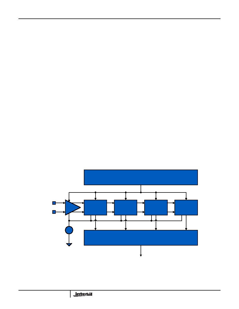
The KAD5512HP is based upon a 12-bit, 250MSPS A/D
converter core that utilizes a pipelined successive
approximation architecture (Figure 21). The input voltage is
captured by a Sample-Hold Amplifier (SHA) and converted
to a unit of charge. Proprietary charge-domain techniques
are used to successively compare the input to a series of
reference charges. Decisions made during the successive
approximation operations determine the digital code for each
input value. The converter pipeline requires six samples to
produce a result. Digital error correction is also applied,
resulting in a total latency of eight and one half clock cycles.
This is evident to the user as a time lag between the start of
a conversion and the data being available on the digital
outputs.
The KAD5512HP family offers 2.5dB improvement in SNR
over the KAD5512P by simultaneously sampling the input
signal with two ADC cores in parallel and summing the digital
result. Since the input signal is correlated between the two
cores and noise is not, an increase in SNR is achieved. As a
result of this architecture, indexed SPI operations must be
executed on each core in series. Refer to “Indexed Device
Configuration/Control” on page 24 for more details.
Power-On Calibration
The ADC performs a self-calibration at start-up. An internal
power-on-reset (POR) circuit detects the supply voltage
ramps and initiates the calibration when the analog and
digital supply voltages are above a threshold. The following
conditions must be adhered to for the power-on calibration to
execute successfully:
A frequency-stable conversion clock must be applied to
the CLKP/CLKN pins
DNC pins (especially 3, 4 and 18) must not be pulled up or
down
SDO (pin 66) must be high
RESETN (pin 25) must begin low
SPI communications must not be attempted
A user-initiated reset can subsequently be invoked in the
event that the previous conditions cannot be met at
power-up.
The SDO pin requires an external 4.7k
Ω pull-up to OVDD. If
the SDO pin is pulled low externally during power-up,
calibration will not be executed properly.
After the power supply has stabilized the internal POR
releases RESETN and an internal pull-up pulls it high, which
starts the calibration sequence. If a subsequent
user-initiated reset is required, the RESETN pin should be
connected to an open-drain driver with a drive strength of
less than 0.5mA.
FIGURE 21. ADC CORE BLOCK DIAGRAM
DIGITAL
ERROR
CORRECTION
SHA
1.25V
INP
INN
CLOCK
GENERATION
2.5-BIT
FLASH
6-STAGE
1.5-BIT/STAGE
3-STAGE
1-BIT/STAGE
3-BIT
FLASH
LVDS/LVCMOS
OUTPUTS
+
–
KAD5512HP
发布紧急采购,3分钟左右您将得到回复。
相关PDF资料
KAD5512P-17Q72
IC ADC 12BIT 170MSPS SGL 72-QFN
KAD5514P-12Q72
IC ADC 14BIT 125MSPS SGL 72-QFN
KAD5610P-25Q72
IC ADC 10BIT 250MSPS DUAL 72-QFN
KAD5612P-17Q72
IC ADC 12BIT 170MSPS DUAL 72-QFN
LA72715NV-TLM-E
IC AUDIO DECODER JPN MTS 24SSOP
LICAL-DEC-LS001
IC DECODER LOW SECURITY 8DIP
LICAL-DEC-MS001
IC DECODER MS SERIES 20-SSOP
LICAL-ENC-MS001
IC ENCODER MS SERIES 20-SSOP
相关代理商/技术参数
KAD5512HP-21Q48
功能描述:模数转换器 - ADC 12-BIT 210MSPS HI PERF SINGLE ADC PROG
RoHS:否 制造商:Texas Instruments 通道数量:2 结构:Sigma-Delta 转换速率:125 SPs to 8 KSPs 分辨率:24 bit 输入类型:Differential 信噪比:107 dB 接口类型:SPI 工作电源电压:1.7 V to 3.6 V, 2.7 V to 5.25 V 最大工作温度:+ 85 C 安装风格:SMD/SMT 封装 / 箱体:VQFN-32
KAD5512HP-21Q72
功能描述:模数转换器 - ADC 12-BIT 210MSPS HI PERF SINGLE ADC PROG
RoHS:否 制造商:Texas Instruments 通道数量:2 结构:Sigma-Delta 转换速率:125 SPs to 8 KSPs 分辨率:24 bit 输入类型:Differential 信噪比:107 dB 接口类型:SPI 工作电源电压:1.7 V to 3.6 V, 2.7 V to 5.25 V 最大工作温度:+ 85 C 安装风格:SMD/SMT 封装 / 箱体:VQFN-32
KAD5512HP-25Q48
功能描述:模数转换器 - ADC 12-BIT 250MSPS HI PERF SINGLE ADC
RoHS:否 制造商:Texas Instruments 通道数量:2 结构:Sigma-Delta 转换速率:125 SPs to 8 KSPs 分辨率:24 bit 输入类型:Differential 信噪比:107 dB 接口类型:SPI 工作电源电压:1.7 V to 3.6 V, 2.7 V to 5.25 V 最大工作温度:+ 85 C 安装风格:SMD/SMT 封装 / 箱体:VQFN-32
KAD5512HP-25Q72
功能描述:模数转换器 - ADC 12-BIT 250MSPS HI PERF SINGLE ADC
RoHS:否 制造商:Texas Instruments 通道数量:2 结构:Sigma-Delta 转换速率:125 SPs to 8 KSPs 分辨率:24 bit 输入类型:Differential 信噪比:107 dB 接口类型:SPI 工作电源电压:1.7 V to 3.6 V, 2.7 V to 5.25 V 最大工作温度:+ 85 C 安装风格:SMD/SMT 封装 / 箱体:VQFN-32
KAD5512P
制造商:INTERSIL 制造商全称:Intersil Corporation 功能描述:Low Power 12-Bit, 250/210/170/125MSPS ADC
KAD5512P_09
制造商:INTERSIL 制造商全称:Intersil Corporation 功能描述:Low Power 12-Bit, 250/210/170/125MSPS ADC
KAD5512P-12Q48
功能描述:模数转换器 - ADC 12-BIT 125MSPS SINGL ADC PROG LVDS/LVCMOS RoHS:否 制造商:Texas Instruments 通道数量:2 结构:Sigma-Delta 转换速率:125 SPs to 8 KSPs 分辨率:24 bit 输入类型:Differential 信噪比:107 dB 接口类型:SPI 工作电源电压:1.7 V to 3.6 V, 2.7 V to 5.25 V 最大工作温度:+ 85 C 安装风格:SMD/SMT 封装 / 箱体:VQFN-32
KAD5512P-12Q72
功能描述:模数转换器 - ADC 12-BIT 125MSPS SINGL ADC PROG LVDS/LVCMOS RoHS:否 制造商:Texas Instruments 通道数量:2 结构:Sigma-Delta 转换速率:125 SPs to 8 KSPs 分辨率:24 bit 输入类型:Differential 信噪比:107 dB 接口类型:SPI 工作电源电压:1.7 V to 3.6 V, 2.7 V to 5.25 V 最大工作温度:+ 85 C 安装风格:SMD/SMT 封装 / 箱体:VQFN-32